ASCII
is a code used to establish a correspondence between letters of the alphabet, numbers 0 through 9, punctuation marks and the corresponding binary number. Here are some examples taken from the ASCII code:|
ASCII |
BINARY |
DECIMAL |
|
A |
01000001 |
65 |
|
B |
01000010 |
66 |
|
C |
01000011 |
67 |
|
D |
01000100 |
68 |
|
E |
01000101 |
69 |
|
F |
01000110 |
70 |
|
0 |
00110000 |
48 |
|
1 |
00110001 |
49 |
|
2 |
00110010 |
50 |
|
3 |
00110011 |
51 |
|
: |
00111010 |
58 |
|
( |
00101000 |
40 |
|
) |
00101001 |
41 |
In practice, the ASCII code is used in the computer keyboard, when for example pressing the A generates the binary number 01000001 equal to 65 decimal.
It is said logic circuit an electric circuit able to realize electrically a logical expression. A combinational circuit is said when the output depends on the combination of inputs in that moment according to a suitable law. The basic logic gates are AND OR NOT
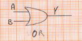
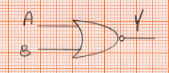
OR LOGIC GATE
The symbol of the OR logic gate is the following:
inputs can be more than two. The OR logic gate follows the following law: the output is at logic level 1 when at least one of the inputs is at logic level 1. The logical expression is as follows: Y = A + B. Truth table is as follows :
|
A |
B |
Y |
|
0 |
0 |
0 |
|
0 |
1 |
1 |
|
1 |
0 |
1 |
|
1 |
1 |
1 |
remember that it is said truth table for a table that shows all possible combinations of inputs that must be the value of the output. In our case, Y is the output.
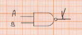
AND LOGIC GATE
The symbol of the AND logic gate is the following:
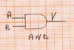
inputs can be more than two. The AND logic gate follows the following law: the output is at logic level 1 when all inputs are at logic level 1. Logical expression is as follows: Y = A x B. Truth table is as follows:
|
A |
B |
Y |
|
0 |
0 |
0 |
|
0 |
1 |
0 |
|
1 |
0 |
0 |
|
1 |
1 |
1 |
NOT LOGIC GATE
The symbol of the NOT logic gate is the following:
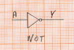
The input is just one. The NOT logic gate follows the following law: the output is at a logic level opposite to that of the input. That is, if the input is 0, the output is 1 and vice versa. The logical expression is as follows: Y = A that is A is denied. The truth table is the following:
|
A |
Y |
|
0 |
1 |
|
1 |
0 |
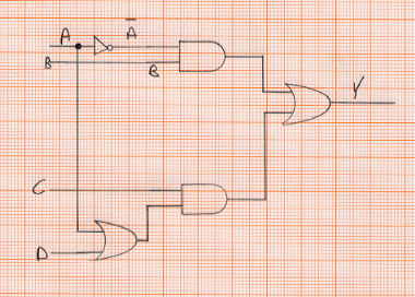
One way to switch from a logic equation to the respective circuit with the logic gates is to replace the + with a logic gate of the OR type and the sign x with a logic gate of the AND type. Given the following equation:
Y =
A x B + C x ( D + A)It starts by drawing on the right an OR gate with two inputs:
upper input is applied the output of one AND whose inputs are A and B, of course necessary a NOT to achieve A:
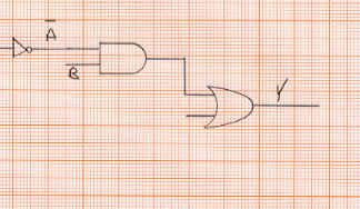
on the second input of the OR final should bring the output of one AND whose inputs will be C and the output of an OR having as inputs D and A. The complete circuit becomes:
To solve a generic problem of logical type must first identify all the variables from which depends the solution and place them in correspondence with a letter of the alphabet A, B, C. Subsequently necessary to build a truth table in which for all combinations of the variables input the output has value 0 or 1, it is logical according to the type of problem proposed.
Example
Consider a vending machine that give consent gasoline power pump, when you reach the amount of € 10.00, both with a € 10 banknote that with two banknotes from 5 €.
Solution
It assigns to input A value of 0 if the € 10 banknote was not included; the value 1 if the € 10 banknote has been inserted. It assigns the value 0 to the variable B if the € 5 banknote was not included, the value 1 if the € 5 banknote has been inserted. Is assigned to the variable C the value 0 if the € 5 banknote was not included, the value 1 if the € 5 banknote has been inserted. The truth table will be the following:
|
A |
B |
C |
Y |
|
0 |
0 |
0 |
0 |
|
0 |
0 |
1 |
0 |
|
0 |
1 |
0 |
0 |
|
0 |
1 |
1 |
1 |
|
1 |
0 |
0 |
1 |
|
1 |
0 |
1 |
1 |
|
1 |
1 |
0 |
1 |
|
1 |
1 |
1 |
1 |
Analyzing the truth table look at the column of the output Y, omit the first 3 values in which the output is 0 and the next we see where the output is 1, and write the equation as the sum of products:
Y =
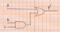
ABC +AB C +ABC+ABC+ABCWe note that if the input variable has a value of 1 is not the negation, if it takes the value 0 must make the denial. To realize such a circuit is required OR to 5 inputs on each of which is applied a three-input AND with any NOT, as explained earlier. Let's say that there are no special procedures for simplification of the equation, which we neglect. However, given our particular problem to be solved, if we neglect the problem of the rest for bills paid any more, we can say, looking at row 5 and 6 of the table that said the consent may be given when the two bills were introduced by € 5, or looking at the last four lines that indicate that only a € 10 note regardless of whether the customer has paid in excess of € 5 banknotes, the equation can be reduced to the following:
Y = A + BC
And then the circuit becomes the following:
The following NAND and NOR gates are the negation of the respective OR gates and AND.
NOR LOGIC GATE
The symbol of the NOR logic gate is the following:
inputs can be more than two. The NOR logic gate follows the following law: the output is at logic level 0 when at least one of the inputs is at logic level 1. The logical expression is the following: Y = A+B. The truth table is the following :
|
A |
B |
Y |
|
0 |
0 |
1 |
|
0 |
1 |
0 |
|
1 |
0 |
0 |
|
1 |
1 |
0 |
NAND LOGIC GATE
The symbol of the NAND logic gate is the following:
inputs can be more than two. The NAND logic gate follows the following law: the output is at logic level 0 only when all inputs are at logic level 1. Logical expression is as follows: Y = AxB. Truth table is as follows :
|
A |
B |
Y |
|
0 |
0 |
1 |
|
0 |
1 |
1 |
|
1 |
0 |
1 |
|
1 |
1 |
0 |
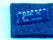
Logic gates integrated circuits of which we see a specimen in the following image:
belong to two basic families:
TTL,
which is made with BJT transistorsCMOS,
which is made with CMOS transistors
POWER SUPPLY
The TTL family has a supply tension of 5 V; instead the family has CMOS supply tension ranging from 5 V and 15 V
PROPAGATION DELAY
The logic gates have a certain delay between the instant in which is applied the input signal and the instant in which the output adapts to the state of the inputs. The greater the delay time the lower the working frequency of the logic gates.
FAN OUT
It is said FAN OUT the maximum number of logic gates that can be connected on the output of a logic gate, in order to withdraw the state; this is due to the fact that each input of a logic gate absorbs a certain current, which must be supplied from the exit of the previous door. For the family TTL the FAN OUT is equal to 1; for family CMOS the FAN OUT is equal to 50, that is you can connect up to 50 ports.
2014